Boosting Semiconductor Yields: Launches High-Efficiency UV Tape Debonding System for Wafer Dicing and Grooving
Introduction: As semiconductor wafers become thinner and more highly integrated, controlling production yields during dicing, grooving, and back-grinding processes has become a critical challenge for the industry. To address this, Shenzhen Super-curing Opto-Electronic CO., Ltd a leading innovator in ultraviolet curing technology, has officially launched its next-generation High-Efficiency Semiconductor UV Tape Debonding System. Designed specifically for advanced semiconductor back-end packaging, this system solves the challenge of peeling high-tack UV dicing tapes without damaging ultra-thin dies, significantly boosting wafer dicing yields and accelerating manufacturing efficiency.
The Semiconductor Pain Point: The "Peeling" Challenge of Ultra-Thin Wafers
During wafer thinning, dicing, and laser grooving, UV dicing tapes (UV Tape) are essential for securely holding the wafer in place to prevent micro-die displacement or cracking. However, once the dicing process is complete, removing these high-tack tapes safely, cleanly, and without causing mechanical stress is a major hurdle:
-
Incomplete Debonding: Standard UV lamps often lack the uniform penetration required to trigger a full reaction in the photoinitiators of high-tack UV adhesives. This results in residual stickiness, leading to die cracking, chipping, or scratching during physical peeling.
-
Thermal Damage & Warpage: Traditional high-pressure mercury lamps generate excessive infrared heat. This thermal stress can cause ultra-thin wafers to warp or delaminate, severely degrading final product yields.
-
Throughput Bottlenecks: Uneven light distribution and long irradiation times create significant bottlenecks in automated semiconductor assembly lines.
Core Advantages: Precise 365nm Wavelength Meets True Cold-UV Technology
Engineered to overcome these industry bottlenecks, Shenzhen Super-curing Opto-Electronic CO., Ltd’s R&D team has optimized the optical structures and curing mechanisms to deliver a high-precision UV-LED debonding solution.
1. Targeted 365nm Peak Wavelength for Instantaneous De-pinning
The system utilizes high-purity, high-output 365nm single-wavelength UV-LED light sources. This precise wavelength perfectly matches the absorption spectrum of photoinitiators found in premium semiconductor UV tapes (such as PO or PVC-based dicing tapes). The UV light instantly penetrates the film base to cross-link the adhesive layer, dropping the tape's peel strength to near-zero within seconds for effortless, residue-free removal.
2. Advanced "Cold Light Source" Optical Architecture
Equipped with a proprietary micro-lens array and a highly efficient thermal management system, this equipment completely eliminates the infrared heat associated with traditional UV curing. Even during continuous high-intensity operation, the wafer surface temperature rise is strictly controlled with ≤ 5°C. This protects ultra-thin wafers (down to 50µm or less) from thermal warpage and performance drift.
3. >95% Irradiance Uniformity Ensures Maximum Die Yield
Through customized optical lens optimization, the system achieves a light intensity uniformity of over 95% across the entire exposure area. Ensuring that every single die on the wafer receives identical UV dosage eliminates localized adhesive residuals or incomplete debonding. This minimizes chipping and die-flying during the subsequent pick-and-place process, maximizing total backend manufacturing yields.
Smart Automation Integration for Modern Wafer Fabs
Beyond its optical performance, the High-Efficiency UV Tape Debonding System features advanced smart control capabilities. It supports standard PLC industrial communication protocols, allowing seamless integration into automated de-tapers, wafer dicing saws, and other automated backend equipment.
The system also includes real-time closed-loop UV intensity monitoring. Operators can dynamically adjust radiation energy and exposure time based on different brands and thicknesses of UV tapes, ensuring absolute process consistency across batches.
Empowering Advanced Packaging Workflows
"The semiconductor packaging and testing industry demands near-zero tolerance for component stress and process instability," stated the Head of R&D at Shenzhen Super-curing Opto-Electronic CO., Ltd. “Our specialized UV tape debonding system is the result of deep research into advanced electronic materials. It not only helps wafer fabs reduce mechanical loss and boost dicing yields, but it also serves as a highly reliable, cost-effective alternative to expensive imported systems."
The system has already successfully passed rigorous line-qualification testing at several leading OSATs (Outsourced Semiconductor Assembly and Test) and wafer foundries, and is now moving into full commercial production.
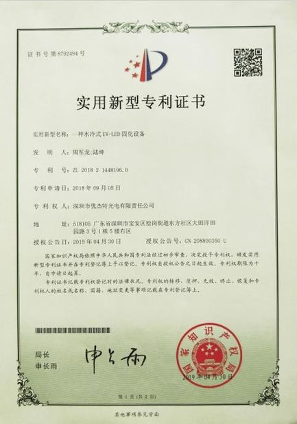
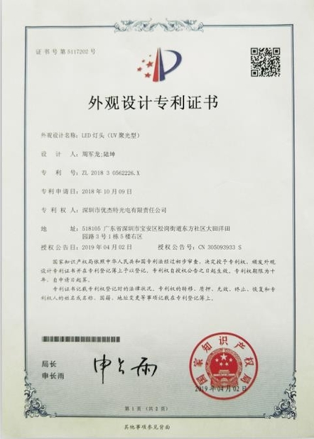
Shenzhen Super-curing Opto-Electronic CO., Ltd is a high-tech enterprise dedicated to the R&D, manufacturing, and distribution of premium ultraviolet curing systems. Holding multiple core patents, our product portfolio includes UV-LED spot, line, and flood curing systems, as well as industrial mercury systems and automated conveyor solutions utilized across the semiconductor, consumer electronics, medical device, and precision printing industries.

 Your message must be between 20-3,000 characters!
 English